Irradiation of Spider Silk
Bruce Wei
Spider silk is used at the Laboratory for Laser Energetics in University of Rochester to hold targets while filling for inertial confinement fusion. When filling the targets with tritium, there will be a certain amount of radiation to the spider silk. The goal is to figure out what happens to spider silk’s physical and chemical properties after irradiation. Our job is to irradiate and then figure out what doses we have given to the silk.
Experimental set up:
Tritium is a beta emitter. This spider silk is radiated by electrons with energies ranging from roughly 2 to 20 keV. Using a Scanning Electron Microscope (SEM), we can expose spider silk to an electron beam to simulate this. Geneseo’s Aspex SEM can produce electron beams of 5, 10, and 15 keV.
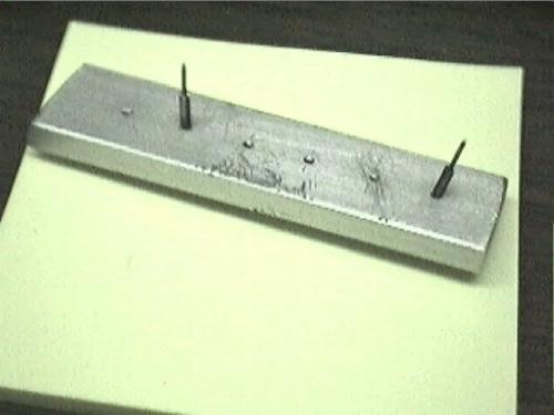
In order to irradiate spider silk, we needed to find a platform that would be compatible with the SEM. That means that it has to be conductive and could not be higher than one centimeter. An aluminum platform, with two metallic pins of approximately 450 µm diameter sticking out, was designed. The spider silk is connected to two small beads about 2 mm long, which slide over the two pins. The distance between two holes in the picture is about 1 inch apart.
This is a picture of the platform with beads on the pins.

| Symbol | Name | Typical value | Comment |
| d | diameter (?m) | 1 | A picture was taken by the SEM and measured using Image J. |
| ? | density (g/cm3) | 1.097 | Obtained fromBonino’s thesis |
| K | average fraction of energy deposited | Seebelow. | |
| Ee | energy per electron (keV) | 5,10,15 | Controlled by the SEM machine |
| I | SEM beam current (nA) | 10-3 – 20 | Main control parameter; higher current gives higher dose.Details here |
| t | time of exposure (s) | Main control parameter; longer time gives higher dose. | |
| L | width of image (mm) | Main control parameter; larger image gives lower dose because a larger fraction of electrons miss the silk. | |
| D | number of dose (rad) |
Determination of K:
When an electron hits the spider silk, it may pass through the silk, only depositing some of its energy there. K is the average fraction of energy deposited, which describes how much energy from the beam current is deposited onto the spider silk. This is very difficult to measure experimentally. We tried using these two software packages to investigate this: CASINO and PENELOPE.
Summary results:
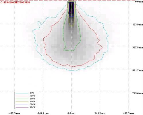
Using CASINO, we simulated electrons hitting an aluminum surface covered with a layer of spider silk material (1 micron thick, similar to the 1 micron diameter of real silk). The images below indicate how the deposited energy is distributed. 5 keV electrons all stop within the spider silk, depositing all of their energy. 15 keV electrons mostly pass through the spider silk, on average depositing only 22% of their energy in the silk.
Energy deposition of various electron beams.
NOTE: Scale is different in the three images. The horizontal dashed line indicates the slik-aluminum boundary (which is below the bottom of the 5 keV image).

5 keV
10 keV
15 keV
